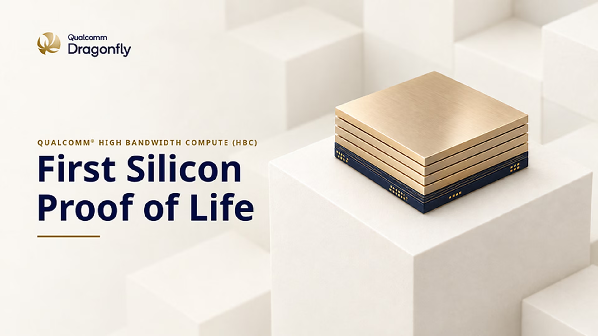
Qualcomm has completed lab testing of the first chips built with its High Bandwidth Compute (HBC) memory technology, the company announced — clearing a key validation milestone on the road to the Dragonfly AI250, per The Next Web.
HBC is Qualcomm's bid to tackle one of the defining bottlenecks in AI infrastructure: moving data to compute fast enough to keep accelerators fed. Passing lab tests doesn't mean the parts are ready to ship, but it does mean the fundamental design works in silicon rather than just on paper — the difference between a roadmap slide and a manufacturable product.
The strategic context matters more than the milestone itself. Qualcomm built its empire on smartphones, and the data-centre AI market is where the industry's capital is currently flooding. The AI250 is the company's vehicle for claiming a slice of that market, and HBC is the differentiator it is betting on to stand out in a field where memory bandwidth increasingly decides which accelerators win deployments.
Validation now shifts the question from "does it work?" to "when does it ship, and at what scale?" Those answers — along with customer commitments — will determine whether HBC becomes a genuine wedge into the data centre or another promising architecture that arrived late to a crowded fight.
Discussion 0
Join the debate — sign in to comment.
Sign inNo comments yet — start the debate.